Electrical Conduction Animation
Introduction
The
conduction of electrical charge in solids is a very complex subject involving
the energy levels of electrons in the solid.
This animation will attempt to simplify that subject.
Electron Reflection by the Atomic Lattice

Figure 1: Electron Reflectance of 75 atomic lattice
planes plotted Vs the electron wave number, k/k0, where k0
is the wave number at the center of the gap.
This would correspond the reflectance of a
nano-crystal that is about 300 Angstroms in length. At low temperatures this
solid is an insulator because its band gap width is essentially quite large. The width of the band gap (called a “stop band” in
optics) is directly proportional on the fractional variation, DV/<V>, of the electric potential in the crystal
lattice.
Figure 1 shows the reflectance of electrons due to the periodic lattice potential variation in a solid. The central Band Gap is between neighboring regions of sidelobes where the Reflectance is less than 1 but often not equal to zero. The number of sidelobes present is equal to the number of lattice planes that were used in the calculation. The envelope of the peaks of these sidelobes does not change when the number of lattice planes in the calculation is increased to infinity. Therefore, even in the energy regions between the stop bands, the electron Transmittance through the lattice is not always equal to 1.0 as is sometimes taught.
In a material where the lattice planes are less distinct and
the lattice plane spacing is therefore somewhat randomized, the Reflectance
function will resemble Figure 1 but central stop band will have less steep
sides and the sidelobes will be “washed out” so that there will be no perfect
nulls but the envelope will still
resemble Figure 1. Otherwise there could
be no amorphous insulators like SiO2.
Discussion of a semi-classical picture
When a substance condenses from a vapor, where the atoms are largely un-ionized, to a solid the spacing between atoms changes drastically. This causes some of the most weakly bound (valence) electrons to be released from the outer shell of the atom. These electrons would, at first, seem to be free to randomly go anywhere within the bounds of the solid. However, because the positive ions remain relatively fixed in their crystal lattice positions, the residual background potential energy of the solid varies periodically in all 3 dimensions as indicated in equation 1.
![]() (1)
(1)
In an insulator, this periodic variation has a large fractional value DV/V in all directions, r. The width of the electron reflectance band gap in Figure 1 is directly proportional to the magnitude of DV/<V>. Therefore, when someone tries to accelerate them with an electric field, the electrons in an insulator are simply reflected as shown in the reflectance plot in Figure 1 (the component of their momentum normal to a given group of crystal lattice planes is reversed) by the periodic structure and they make no progress in the direction of the electric field.
In a conductor, the number of ionized electrons is so large that they are able to effectively screen out the periodic positive ion structure of the solid in all but a few directions so that DV/<V>=0 and therefore the reflectance band width in Figure 1 is practically zero. So then the electrons are truly able to roam the entire solid and can respond very well to an electric field.
So, whether DV/<V>
(and the band gap) is small or large really depends strongly on the number of
electrons in the outer shell available to be ionized as well as the distance
between the ions of the positive background lattice. A large density of ionized electrons or a
small distance between ions results in good screening and a conductor. For a
small density of ionized electrons or large distances between ions we would
expect an insulator. All this is changed drastically by the
quantum nature of the electrons, particularly their adherence to the Pauli
Exclusion Principle, as will be discussed next.
Discussion of the quantum picture
It is a fact of nature that, as a result of the quantum nature of the atoms in the condensed state, all of the outer shell (valence) electrons become ionized, which leads to drastic differences from the classical picture. We use the term “energy band” to describe the energy distributions of these ionized electrons and the band in which they’re located is usually called the “conduction band”.
Next we have to consider the possible quantum states that these electrons might occupy. It turns out that the electrons’ domain becomes the entire extent the solid object in which they reside. The wave functions of these electrons have to be zero at the solid’s boundaries but, other than that, they are simple sinusoids. In addition to this, since the electrons have absolute spin ½ and are therefore Fermions, all the spatial wave functions have to be different except that we can have 2 electrons, one of spin +½ and the other of spin –½ occupying each spatial wave function.
So, if we have 2 (or an even number of) valence electrons per atom, these will fill all possible spatial wave functions as well as both spin states. In this case, the conduction band is full and, if DV/<V>, the fractional crystal potential that the electrons see is large, then the electrons at the top of the band are just reflected back and forth by this crystal potential and can’t be accelerated by an electric field (recall that, if electrons with energy below the top of the band are accelerated, they would occupy the wave function of some other electron pair and this is not permitted). This is the case for what we call an insulator.
On the other hand, if DV/<V> is smaller, then some of the electrons at the top of the conduction band can be thermally excited sufficiently that they are promoted to the next higher band, where their net energies (and momenta) are low enough that they no longer are reflected from the next stop band of the periodic DV/<V> variation. These can then be accelerated by an electric field so that some small conduction occurs. This is the situation that we call a semiconductor. A semiconductor is an insulator at 0 degrees Kelvin since there is no thermal energy at this temperature to promote the electrons to the next higher band.
The other very important case is a solid with only 1 (or an odd number) of valence electrons per atom. Since there can be twice as many electrons in this solid’s uppermost band as we actually have available, this solid’s conduction band is only half full and therefore the electrons do not interact with the periodic DV/<V>. Therefore, an electric field can easily increase the energy of the most energetic of the electrons in this solid and it becomes a conductor.
In a real three dimensional solid, the situation is somewhat more complicated than expressed here because the period of DV/<V> changes with electron momentum direction so that there are many important values of momentum where the electron Reflectance function is maximized. So, for example, the average occupancy of the conduction band of a conductor-like solid could vary from 0.1 to 0.9 and the solid would still be a good conductor.
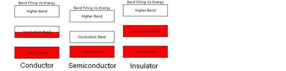
Figure 2. Schematic diagram of the electron band occupation Vs energy (on the
vertical axis) for three different types of solids at 0 degrees Kelvin. The red regions are the occupied regions of
the bands. Note that the semiconductor’s

Figure 3. Schematic diagram of the electron band occupation Vs energy (on the
vertical axis) for three different types of solids at 300 degrees Kelvin. The red regions are the occupied regions of
the bands. The above diagram shows some
fuzziness of the electrons at the tops of the occupied regions. This is due to
finite temperature. At this higher
temperature there are now some electrons in the conduction band of the
semiconductor and therefore it becomes somewhat conductive.
In Figure 3 we see that there are some thermal electrons occupying the gap between the insulator’s conduction band and its higher band. Even though these electrons occupy the gap, it is impossible to accelerate them because they are in the stop band where the electron Reflectance is 1.0.
Discussion of the animation

Figure 4: Animation model. As shown, the electrons are red and the ions
are blue and much larger than the electrons.
The Figure includes a wire between the ends of the solid as well as a
voltage supply in the middle of the wire.
Figure 4 depicts the electrons for a conductor so the total number of red electrons in the rectangular region at the top is the same as the number of blue ions there. In the case of an insulator, where the ions are doubly ionized, the number of electrons is twice that of the ions. In addition, the animation shows that the range of motion of electrons in the conductor is the entire rectangular area but the motion of the electrons in the insulator just back and forth along randomly chosen directions and with randomly chosen amplitudes. The latter motion depicts that the electrons at the top of the conduction band in an insulator tend to get reflected from the lattice potential variations.
In Figure 4, the electrons in the
“wire” are evenly distributed because Figure 4 depicts a conductor. But in a semiconductor, the electrons in the
“wire” are both fewer and randomly distributed in order to depict the fact that
the conduction of a semiconductor is lower as well as more thermally dominated
than that in a conductor.